- 您现在的位置:买卖IC网 > Sheet目录322 > DS2045Y-70# (Maxim Integrated)IC NVSRAM 1MBIT 70NS 256BGA
�� �
�
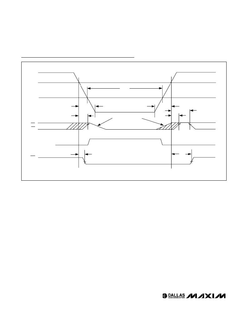
�DS2045Y/AB� Single-Piece� 1Mb�
�Nonvolatile� SRAM�
�Power-Down/Power-Up� Condition�
�V� CC�
�V� TP�
�t� DR�
�~2.7V�
�t� F�
�t� R�
�t� REC�
�CE,�
�WE�
�BACKUP� CURRENT�
�SUPPLIED� FROM�
�LITHIUM� BATTERY�
�RST�
�t� PD�
�V� OL�
�t� RPD�
�SLEWS� WITH�
�V� CC�
�t� PU�
�t� RPU�
�V� OL�
�V� IH�
�(SEE� NOTES� 1,� 7.)�
�Note� 1:� RST� is� an� open-drain� output� and� cannot� source� current.� An� external� pullup� resistor� should� be� connected� to� this� pin� to� real-�
�ize� a� logic-high� level.�
�Note� 2:� These� parameters� are� sampled� with� a� 5pF� load� and� are� not� 100%� tested.�
�Note� 3:� t� WP� is� specified� as� the� logical� AND� of� CE� and� WE� .� t� WP� is� measured� from� the� latter� of� CE� or� WE� going� low� to� the� earlier� of�
�CE� or� WE� going� high.�
�Note� 4:� t� WR1� and� t� DH1� are� measured� from� WE� going� high.�
�Note� 5:� t� WR2� and� t� DH2� are� measured� from� CE� going� high.�
�Note� 6:� t� DS� is� measured� from� the� earlier� of� CE� or� WE� going� high.�
�Note� 7:� In� a� power-down� condition,� the� voltage� on� any� pin� can� not� exceed� the� voltage� on� V� CC� .�
�Note� 8:� The� expected� t� DR� is� defined� as� accumulative� time� in� the� absence� of� V� CC� starting� from� the� time� power� is� first� applied� by� the�
�user.� Minimum� expected� data-retention� time� is� based� on� a� maximum� of� two� 230� °� C� convection� solder� reflow� exposures,�
�followed� by� a� fully� charged� cell.� Full� charge� occurs� with� the� initial� application� of� V� CC� for� a� minimum� of� 96� hours.� This� para-�
�meter� is� assured� by� component� selection,� process� control,� and� design.� It� is� not� measured� directly� in� production� testing.�
�Note� 9:� WE� is� high� for� a� read� cycle.�
�Note� 10:� OE� =� V� IH� or� V� IL� .� If� OE� =� V� IH� during� write� cycle,� the� output� buffers� remain� in� a� high-impedance� state.�
�Note� 11:� If� the� CE� low� transition� occurs� simultaneously� with� or� latter� than� the� WE� low� transition,� the� output� buffers� remain� in� a� high-�
�impedance� state� during� this� period.�
�Note� 12:� If� the� CE� high� transition� occurs� prior� to� or� simultaneously� with� the� WE� high� transition,� the� output� buffers� remain� in� a� high-�
�impedance� state� during� this� period.�
�Note� 13:� If� WE� is� low� or� the� WE� low� transition� occurs� prior� to� or� simultaneously� with� the� CE� low� transition,� the� output� buffers� remain�
�in� a� high-impedance� state� during� this� period.�
�Note� 14:� DS2045� BGA� modules� are� recognized� by� Underwriters� Laboratory� (UL)� under� file� E99151.�
�6�
�_____________________________________________________________________�
�发布紧急采购,3分钟左右您将得到回复。
相关PDF资料
DS2050W-100#
IC NVSRAM 4MBIT 100NS 256BGA
DS2065W-100#
IC NVSRAM 8MBIT 100NS 256BGA
DS2070W-100#
IC NVSRAM 16MBIT 100NS 256BGA
DS2227-070
IC NVSRAM 4MBIT 70NS 72SIMM
DS2423D/T&R
IC SRAM 4KBIT 6FCHIP
DS2430AP+T&R
IC EEPROM 256BIT 6TSOC
DS2431GA+U
IC EEPROM 1024BIT 2SFN
DS2433X-S#T
IC EEPROM 4KBIT 6FCHIP
相关代理商/技术参数
DS205
功能描述:烙铁 Weller Inline Filter For DS1201ESD/1203A
RoHS:否 制造商:Weller 产品:Soldering Stations 类型:Digital, Iron, Stand, Cleaner 瓦特:50 W 最大温度:+ 850 F 电缆类型:US Cord Included
DS2-05-07-015-JV
制造商:IDEC CORPORATION 功能描述:OBJECT DETECTION AND MEASUREMENT LIGHT GRIDS
DS2-05-07-030-JV
制造商:IDEC CORPORATION 功能描述:957501050 Light grids
DS2-05-07-045-JV
制造商:IDEC CORPORATION 功能描述:957501060 Light grids
DS2-05-07-060-JV
制造商:IDEC CORPORATION 功能描述:957501000 Light grids sensor
DS2-05-07-075-JV
制造商:IDEC CORPORATION 功能描述:OBJECT DETECTION AND MEASUREMENT LIGHT GRIDS
DS2-05-07-090-JV
制造商:IDEC CORPORATION 功能描述:957501010 Light grids
DS2-05-07-105-JV
制造商:IDEC CORPORATION 功能描述:OBJECT DETECTION AND MEASUREMENT LIGHT GRIDS